Brief Summary
This video provides an introduction to Bipolar Junction Transistors (BJTs), covering their construction, operation regions, symbols, configurations, and current relationships. It explains how BJTs can function as switches or amplifiers and highlights the importance of understanding their characteristics for electronics enthusiasts.
- BJTs are three-terminal semiconductor devices that can act as conductors or insulators based on the input signal.
- They have three doped regions: Emitter, Base, and Collector, leading to NPN or PNP transistor types.
- BJTs can operate in Active, Saturation, Cut-off, and Reverse Active regions, each with specific biasing conditions.
- The relationship between Base, Collector, and Emitter currents is crucial for understanding BJT behaviour and amplification.
Introduction
The video introduces the Bipolar Junction Transistor (BJT) as a fundamental semiconductor device that paved the way for integrated circuits and modern electronics. BJTs are three-terminal devices that can operate as either conductors or insulators depending on the input signal. This property allows them to be used as switches in digital electronics or as amplifiers in analogue electronics. While field-effect transistors (FETs) are now widely used, BJTs remain relevant, making a basic understanding of them essential for anyone interested in electronics.
What is BJT?
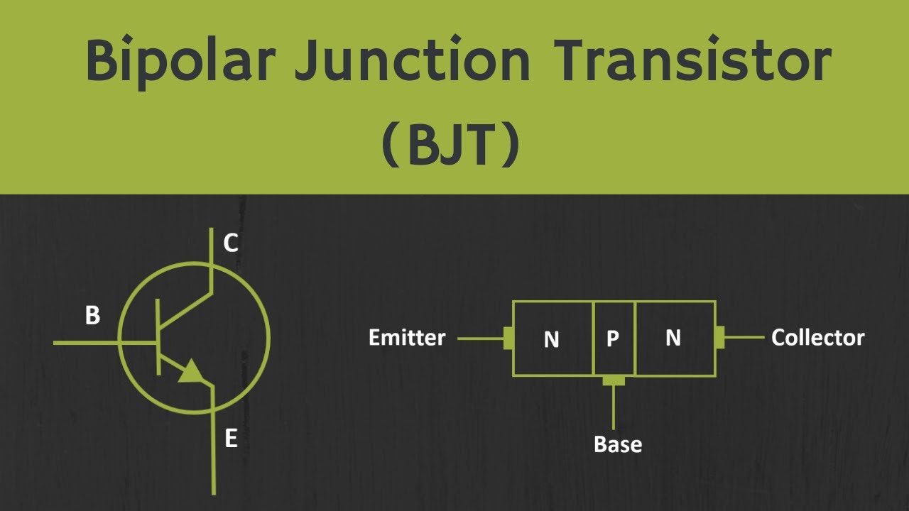
A BJT has three doped regions: the Emitter, the Base, and the Collector. Based on the doping of these regions, a BJT is classified as either an NPN or a PNP transistor. In an NPN transistor, the Emitter and Collector are doped with N-type impurities, while the Base is doped with P-type impurities. Conversely, in a PNP transistor, the Base is doped with an N-type impurity, while the Emitter and Collector are doped with P-type impurities. The term "bipolar" indicates that both electrons and holes contribute to the flow of current within the transistor. Internally, a BJT has two PN junctions: one between the Emitter and the Base, and another between the Base and the Collector.
Construction of BJT
The Emitter is heavily doped to supply electrons, which is why it's called the Emitter. The Base is lightly doped, and the Collector is moderately doped, with a doping concentration between that of the Emitter and the Base. The Base region is much narrower than the Emitter and Collector regions. The Collector region is wider because its job is to collect the electrons supplied by the Emitter, hence the name Collector.
Different Regions of Operation of BJT (Active, Saturation, and Cut-off)
Depending on the biasing, a BJT can operate in three primary regions: the Active Region, the Cut-off Region, and the Saturation Region. In the Active Region, the Emitter-Base junction is forward biased, and the Base-Collector junction is reverse biased. For an NPN transistor to operate in the active region, the Collector voltage (VC) should be greater than the Base voltage (VB), which should be greater than the Emitter voltage (VE). In the Cut-off Region, both the Base-Emitter and Base-Collector junctions are reverse biased. In the Saturation Region, both junctions are forward biased, meaning the Base voltage is greater than both the Emitter and Collector voltages. There is also a Reverse Active Region, where the Base-Collector junction is forward biased and the Base-Emitter junction is reverse biased, but this region is typically avoided due to low gain.
Symbols of NPN and PNP transistor
The symbol for an NPN transistor includes three terminals: Base, Collector, and Emitter. An arrow indicates the direction of current flow during active region operation, flowing from the Base towards the Emitter. The PNP transistor symbol is similar, but the arrow's direction is reversed, indicating current flow from the Emitter towards the Base.
Different Configurations (CE, CB, and CC)
When a BJT is used for signal amplification, it operates in the active region. There are three main configurations: Common Emitter (CE), Common Collector (CC), and Common Base (CB). In the Common Emitter configuration, the Emitter terminal is common to both the input and output. The input signal is applied between the Base and the Emitter, and the output is measured between the Collector and the Emitter. In the Common Collector configuration, the Collector terminal is common between the input and output. In the Common Base configuration, the Base terminal is common between the input and output. Each configuration has its advantages and disadvantages, and the choice depends on the specific application requirements.
Working of BJT
When the BJT operates in the active region, the Base-Emitter junction is forward biased, and the Base-Collector junction is reverse biased. The voltage VBE defines the difference between the voltage at the Base and the Emitter terminal (VB - VE), while VCE is the difference between the Collector and Emitter voltage (VC - VE). When the Base-Emitter junction is forward biased, the typical voltage drop across it is around 0.7 volts. Electrons from the heavily doped Emitter are pushed towards the Base region. Once these electrons enter the Base region, most of them enter into the Collector region due to the Base being lightly doped and very thin. Only a few electrons recombine with holes in the Base region and flow towards the positive terminal of the Base supply. The electrons that enter the Collector region are attracted by the positive terminal of the Collector voltage supply (VCC).
Different Currents in BJT
The Emitter current (IE) is the sum of the Base current (IB) and the Collector current (IC), expressed as IE = IB + IC. Since only a small fraction of electrons flow through the Base, the Collector current (IC) is approximately equal to the Emitter current (IE). The relationship between these currents can be defined as IC = α * IE, where α represents the fraction of the Emitter current flowing through the Collector terminal. The Base current can also be expressed as IB = (1 - α) * IE. The Collector current is also related to the Base current by the equation IC = β * IB, where β is the current gain of the BJT, typically ranging from 50 to 400. The Emitter current can then be expressed as IE = (β + 1) * IB. BJTs are considered current-controlled devices because the Base current controls the Collector current.